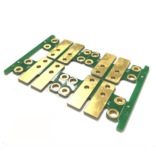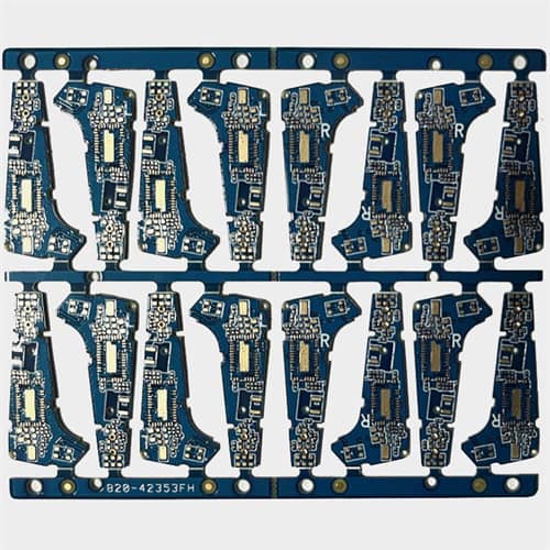

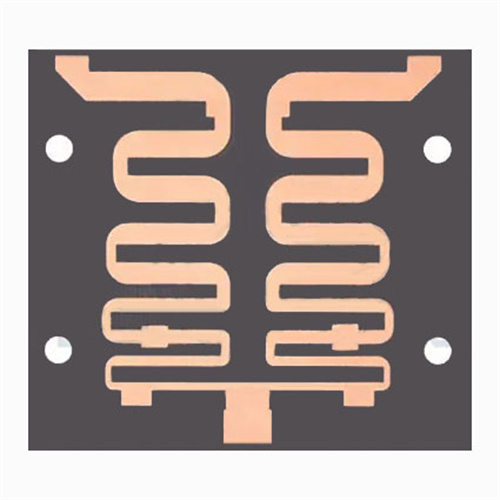
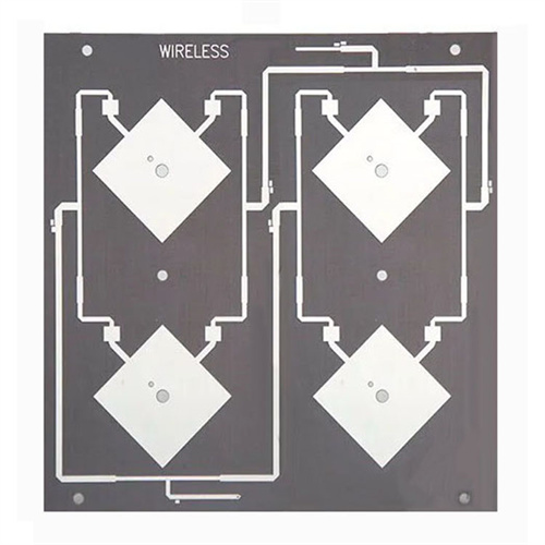
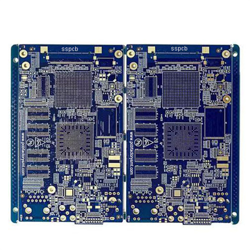
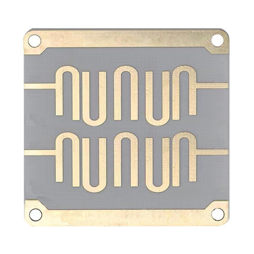
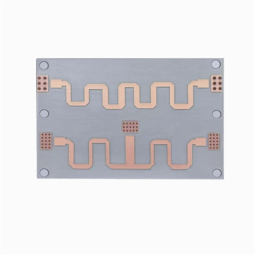
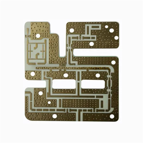
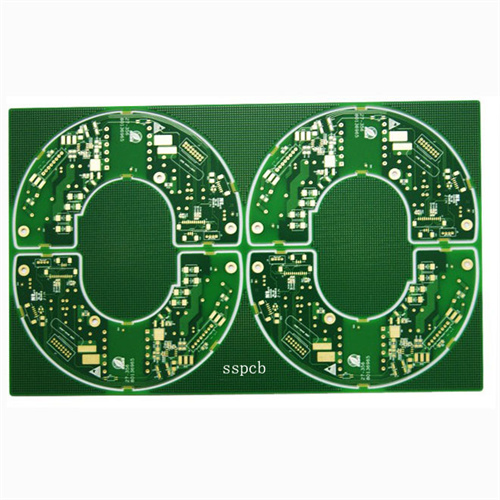
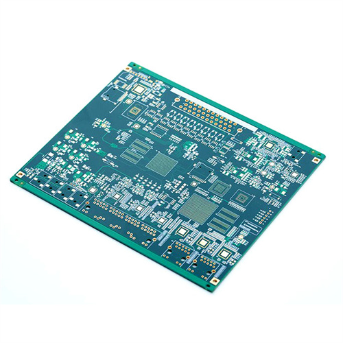
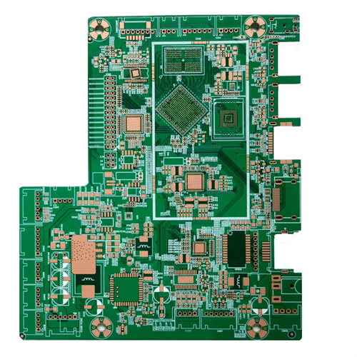
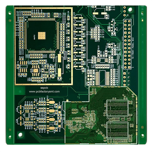
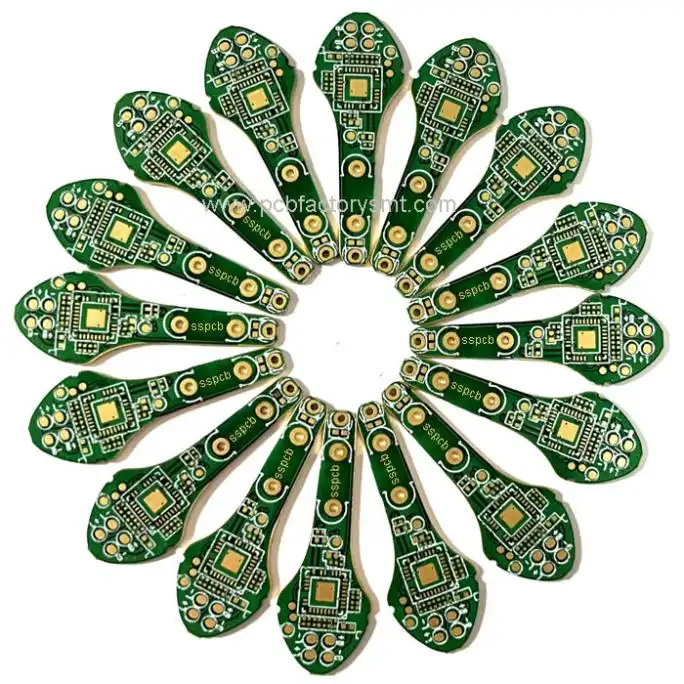
Introduction of 4-Layer PCB
The most important layer of the PCB is the copper foil signal layer, which is the PCB circuit. 4 layers of PCB have 4 circuit layers, and these circuit layers are used to connect other electronic components of the device group.
Technical parameters of 4-Layer PCB
Model: 4 Layer PCB
Material: FR4
Layer: 4 Layers
Color:Green/White/Red/Black
Finished Thickness:0.3-6.0mm
Copper Thickness:0.5OZ-6Z
Surface Treatment Immersion Gold/OSP/lead-free HASL
Min Trace:3mil.0.075mm
Min Space:3mil.0.075mm
Application:Consumer electronics
Layout rules for 4-layer PCB
1. 4-layer PCB in the design of more than 3 points of the connection line, the rules of the yield line should pass through each point in turn, to facilitate later testing, and try to shorten the line length.
2. Avoid wiring around the pins, with special attention to reducing the wiring design between and around the IC pins.
3. Four-layer PCB is best not to route adjacent layers in parallel. Theoretically, as long as the lines are parallel, there will be interference.
4. Minimize bending wiring to avoid electromagnetic radiation.
5. Multi-logic circuit design of ground and power lines at least 10-15mil.
6. Try to connect the ground line multi-segment line to increase the grounding area. Line and line should be kept neat.
7. In the early stage of wiring, space should be reserved for uniform discharge of later components for later installation, plugging and soldering of components. The text is arranged in the current character layer in a reasonable position to avoid being obscured.
8. The placement and installation of components should be considered from the sense of space, and the positive and negative poles of SMT components should be marked at the end of the package.
9. The current 4-layer PCB printed circuit board available thousand 4-5mil wiring, but usually 6mil line width, 8ml line spacing, 12/20MIL pad. Wiring should consider the impact of a variety of factors such as injection current.
10. Functional block components as far as possible together, to facilitate later inspection. Special reminder: zebra strip and other components near the LCD can not be too close.
11. Through-hole coating green oil.
12. 4-layer PCB is best not to put insult pads, over the sub below the battery holder, etc., to ensure the solidity of repeated use.
13. After wiring carefully check whether the wiring is really connected (can use the light method).
14. oscillation circuit components as close as possible to the IC chip, away from the antenna and other vulnerable areas. Grounding pads should be placed below the crystal. 15, consider reinforcement, digging hollow elements and other methods to avoid excessive radiation sources.
FAQ
Q1. What documents do you need to prepare if you want to get a quote from us?
A: PCB boards need to prepare Gerber files, including RS274X, ODB++, DXF, PCB, PCBDOC and other formats.
For PCBA (PCB with soldered components), in addition to the files of PCB, you also need to prepare BOM list (component list), Pick and Place file (txt format), physical sample drawing or 3D PDF version file, etc.
PCB layout requires a PCB schematic and PCB outline drawing.
For PCB design, you need to express your ideas and we will discuss whether we can implement your ideas.
Q2. Do you have a minimum order quantity?
A: We have the flexibility to handle both small and large volume production. We do not have any minimum order quantity, and the smallest order we accept is 1 piece.
In general, the higher the quantity produced, the lower the unit price and the longer the delivery time.
Q3. How can we keep our product information and design documents confidential?
A: Your files are completely safe and secure. We protect the intellectual property of our clients throughout. All files from our clients are never shared with any third party.
Q4. How long is the delivery time?
A: The production time for standard PCB samples is 1-7 days, 7-10 days for small batch production, and 12-25 days for large orders.
For the production of non -standard PCB and PCBA, please send the reference file and production requirements to sales@pcbfactorysmt.com,we will reply to you as soon as possible.
Q5. What are the main products of your PCB / PCBA service?
A: Industrial control, automotive, medical equipment, communication electronics, aviation, LED...
Q6. How long does it take for PCB and PCBA quotation?
A: PCB quotation can be completed within 0.5-2 hours PCBA depends on the number of components, simple can be completed within 6 hours, complex 12-36 hours can be completed.
Q7. Shipping fee?
A: Usually we offer EXW, FCA, FOB, CIF and DDU terms, if there is no special request, the default terms quoted are FOB Shenzhen. Please mention the terms and conditions when you have any request.
We work with courier companies including DHL, FedEx, UPS, TNT and EMS, with air and sea freight also optional.
Shipping costs are determined by the destination, weight, and package size of the shipment. If you need us to quote the shipping cost, please let us know.
Q8. Do you accept process materials from customers?
A: Yes, we can source components and we accept components from our customers.