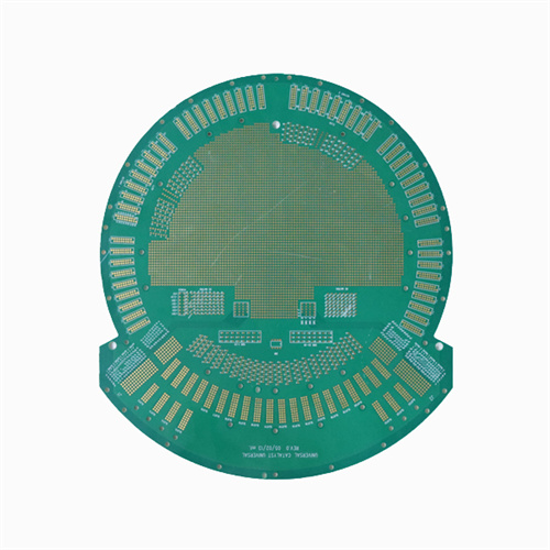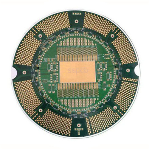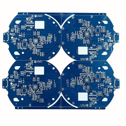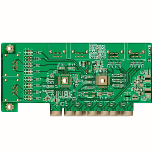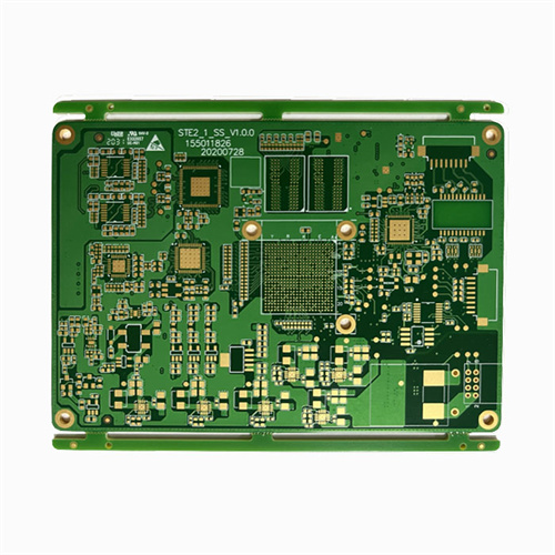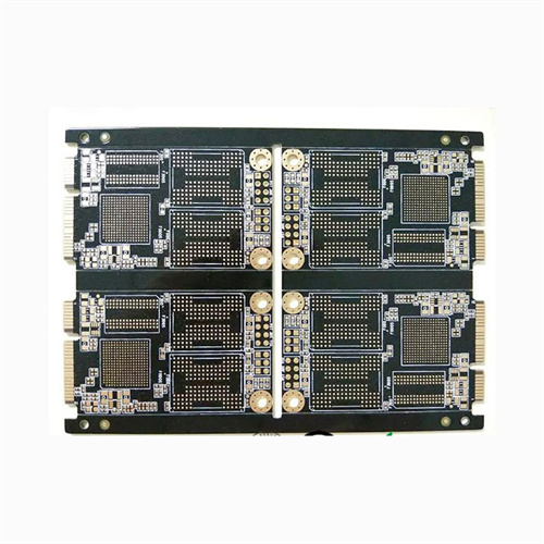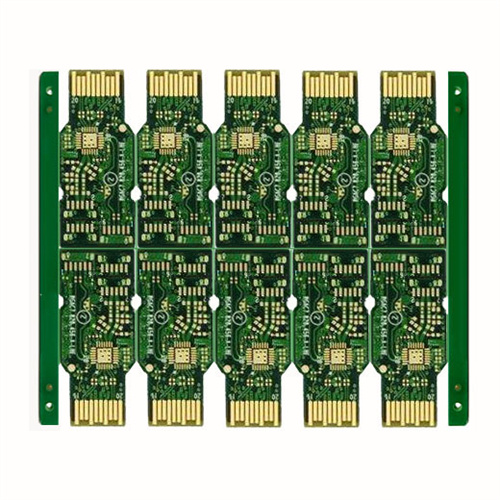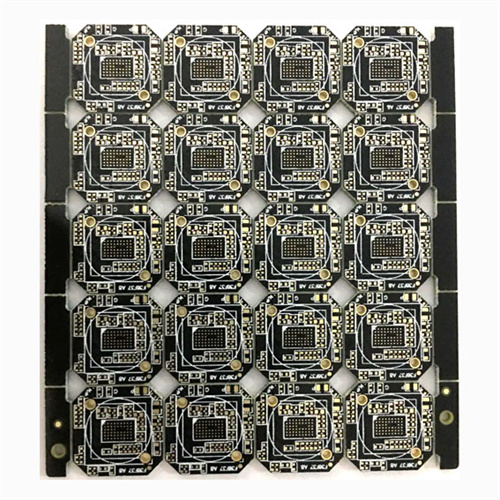
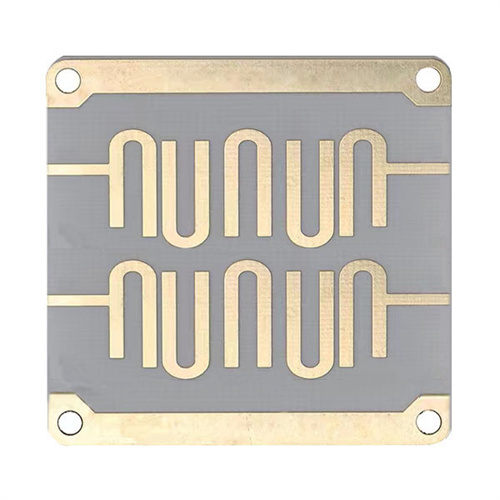
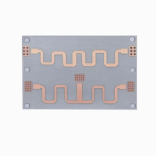
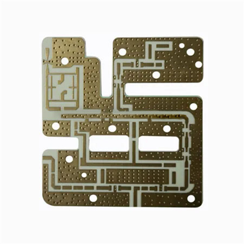
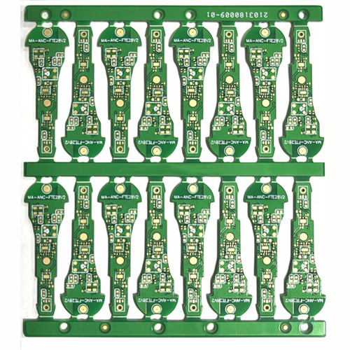
Technical parameters of Halogen-free PCB
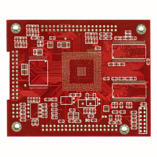
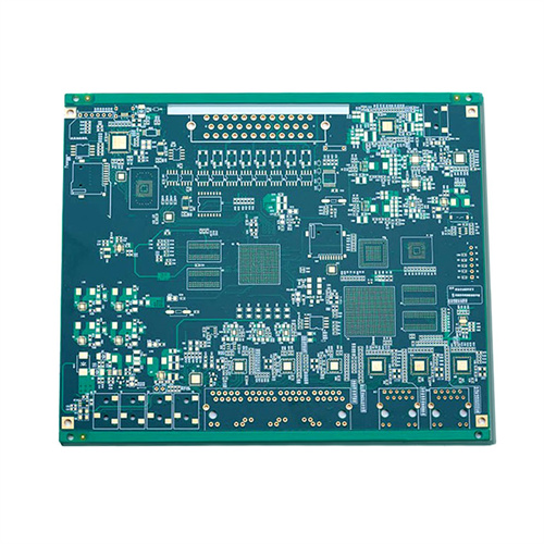
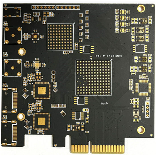
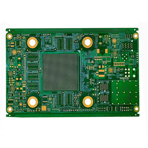
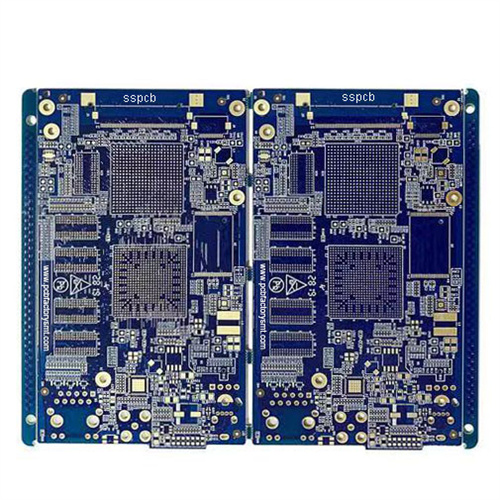
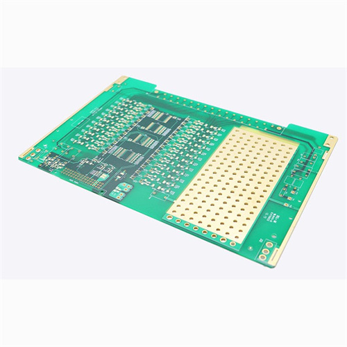
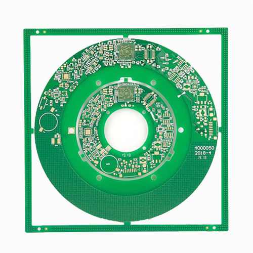
Model:Display Backplane Halogen-Free PCB
Material:S1150G
Layer: 10Layers
Color:Green/White
Finished Thickness:0.8mm
Copper Thickness:0.5Z
Surface Treatment:Immersion Gold
Min Trace:3mil(0.075mm)
Min Space:3mil(0.075mm)
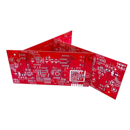
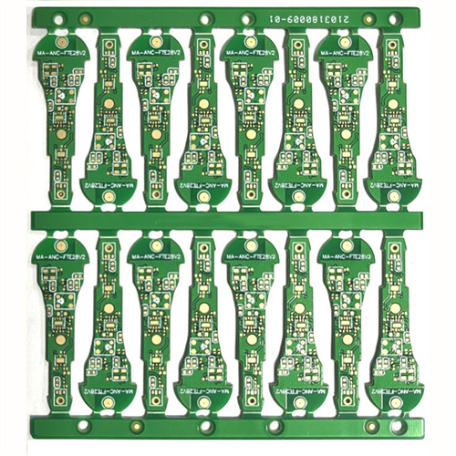
Characteristic: Halogen-free(HF PCB)
Application:Display Backplane Halogen-Free PCB
Features of halogen-free PCB
1.Halogen-free PCB material insulation.
As the halogen atom is replaced by P or N, the polarity of the bonded segment of the epoxy resin molecule is reduced to a certain extent, thus improving the insulation resistance and breakdown resistance quality of the PCB.
2.Halogen-free PCB material water absorption.
Halogen-free sheet has fewer electrons than the halogen in the ammonia-phosphorus-based oxygen reduction resin, and the probability of forming hydrogen bonds with hydrogen atoms in water is lower than that of halogen materials, so the water absorption of the material is lower than that of conventional halogen-based PCB yin-fired materials. For PCB boards, low water absorption rate to improve the reliability and stability of the material has a certain impact.
3.The thermal stability of halogen-free PCB materials.
Halogen-free PCB board in the ammonia and phosphorus content is greater than the halogen content of ordinary halogen materials, so its monomer molecular weight and PCB Tq values are increased. In the case of heat, the mobility of its molecules will be lower than that of conventional epoxy resins, so the coefficient of thermal expansion of halogen-free PCB materials is relatively small.
FAQ
Q1. What documents do you need to prepare if you want to get a quote from us?
A: PCB boards need to prepare Gerber files, including RS274X, ODB++, DXF, PCB, PCBDOC and other formats.
For PCBA (PCB with soldered components), in addition to the files of PCB, you also need to prepare BOM list (component list), Pick and Place file (txt format), physical sample drawing or 3D PDF version file, etc.
PCB layout requires a PCB schematic and PCB outline drawing.
For PCB design, you need to express your ideas and we will discuss whether we can implement your ideas.
Q2. Do you have a minimum order quantity?
A: We have the flexibility to handle both small and large volume production. We do not have any minimum order quantity, and the smallest order we accept is 1 piece.
In general, the higher the quantity produced, the lower the unit price and the longer the delivery time.
Q3. How can we keep our product information and design documents confidential?
A: Your files are completely safe and secure. We protect the intellectual property of our clients throughout. All files from our clients are never shared with any third party.
Q4. How long is the delivery time?
A: The production time for standard PCB samples is 1-7 days, 7-10 days for small batch production, and 12-25 days for large orders.
For the production of non -standard PCB and PCBA, please send the reference file and production requirements to sales@pcbfactorysmt.com,we will reply to you as soon as possible.
Q5. What are the main products of your PCB / PCBA service?
A: Industrial control, automotive, medical equipment, communication electronics, aviation, LED...
Q6. How long does it take for PCB and PCBA quotation?
A: PCB quotation can be completed within 0.5-2 hours PCBA depends on the number of components, simple can be completed within 6 hours, complex 12-36 hours can be completed.
Q7. Shipping fee?
A: Usually we offer EXW, FCA, FOB, CIF and DDU terms, if there is no special request, the default terms quoted are FOB Shenzhen. Please mention the terms and conditions when you have any request.
We work with courier companies including DHL, FedEx, UPS, TNT and EMS, with air and sea freight also optional.
Shipping costs are determined by the destination, weight, and package size of the shipment. If you need us to quote the shipping cost, please let us know.
Q8. Do you accept process materials from customers?
A: Yes, we can source components and we accept components from our customers.