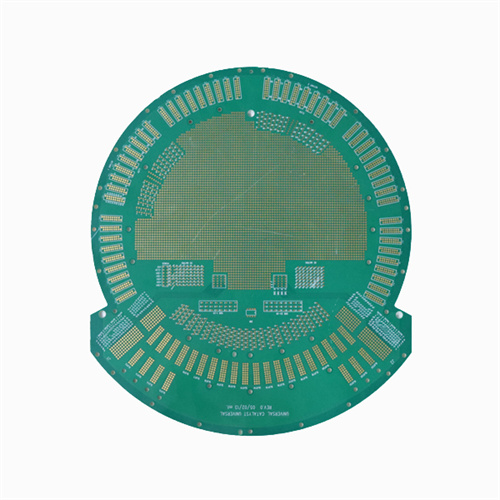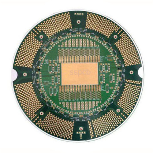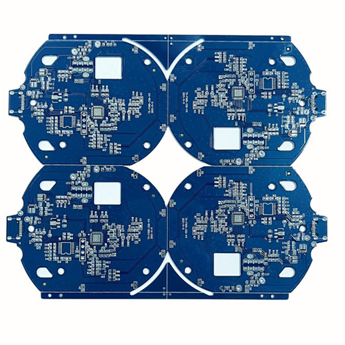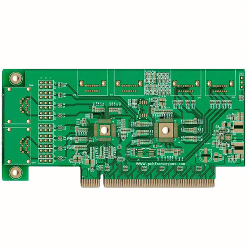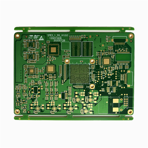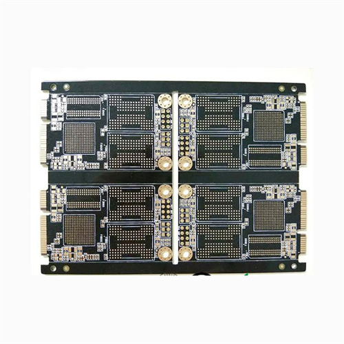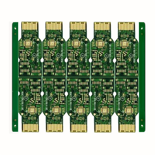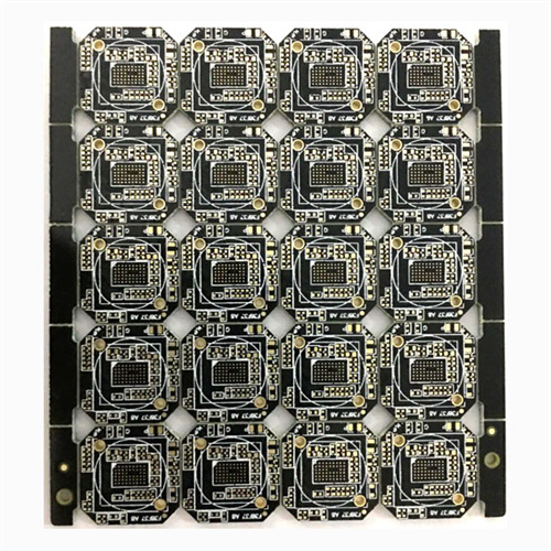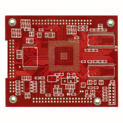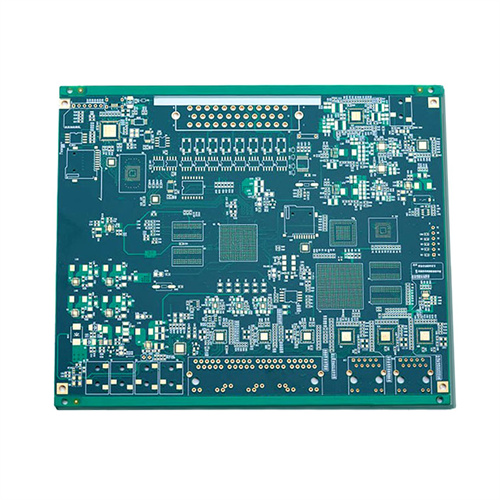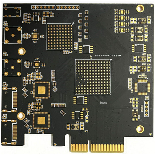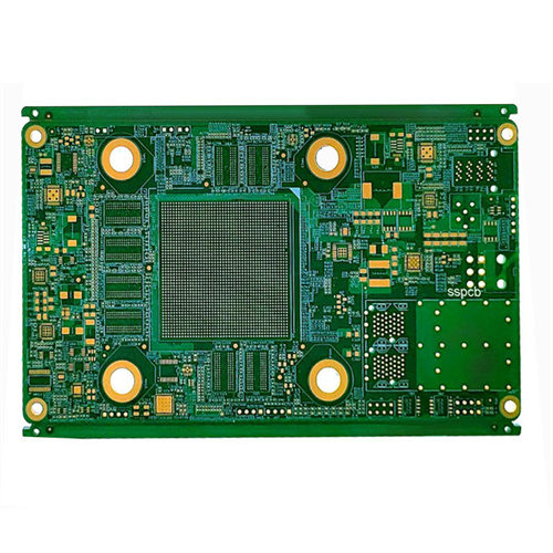
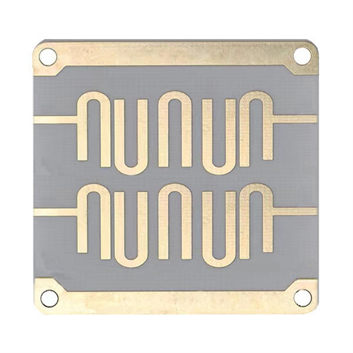
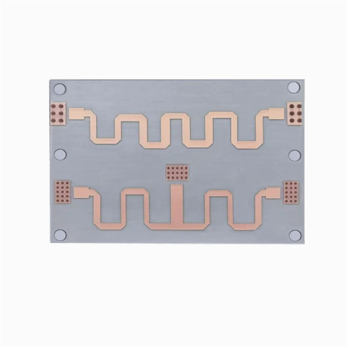
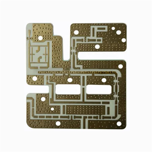
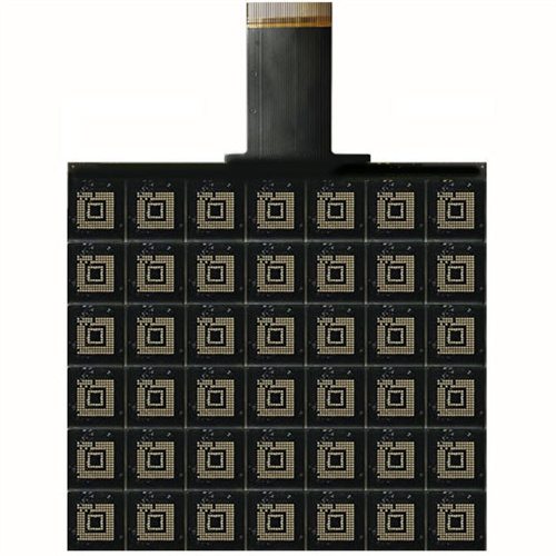
Introduction of Burn-in board
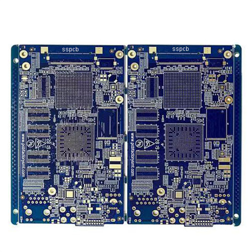
IC aging test board is used as a carrier for semiconductor IC. IC to be tested are connected to the IC aging test board through SOCKET or other means and put into the test machine to test the reliability of IC at different temperatures, voltages and signal lights.
Technical parameters of Burn-in board
Model:Burn-in Board
Material:High TG TG175
Layer: 20Layers Color: Green
Size:610*572mm
Board Thickness:3.2mm
BGA number:24
Surface technology: Immersion Gold(3U)
Copper thickness: inner layer 70/35um. outer layer 35um
Application:IC burn-in test board (BIB) PCB
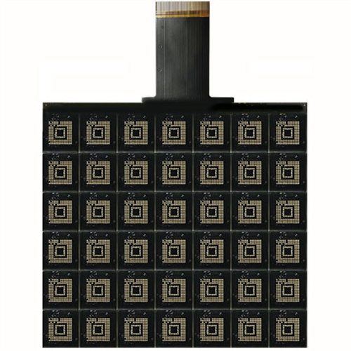
BIB (Burn-In Board) aging test board several requirements
1. In order to prevent the chip power or signal short-circuit caused by other chips can not work, each chip power supply needs to be independent, connected to the main power supply through a resistor.
2. When the alignment current is greater than 500mA, it needs to be marked in the schematic diagram.
3. High frequency wiring such as impedance matching, copper foil thickness, line width and PCB board material should be given.
4. The need for shielding or other special treatment of sensitive ports, devices, etc. need to be clearly marked.
5. The crystal circuit needs to give a typical application circuit, including matching capacitance values.
6, need to indicate whether the analog and digital circuits and tiling need to be separated.
7. If you need to provide an external signal source, please give the driving capacity of the required signal source and related indicators.
8. PCB board long-term in high temperature (150 degrees Celsius) without abnormal deformation or bending.
9. PCB circuit will not have any short circuit or breakage due to high temperature environment.